Home

Wednesday, August 30, 2023

Sony STR-7065 Receiver Restoration

Unit: AM/FM Stereo Receiver
Manufacturer: Sony
Model: STR-7065
SN: 818755

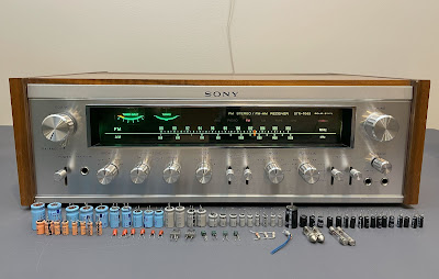
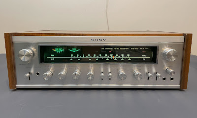
Today I'm showing a vintage Sony STR-7065 receiver that came in for restoration. This model was manufactured from 1972 to 1974. It delivers 60 watts per channel into 8 ohms with a total harmonic distortion of no more than 0.2%. The damping factor at 8 ohms is 50. The retail price in 1973 was $459.50 (Ref. High Fidelity, May 1973, page 30). A very good review of this model was published a year later in High Fidelity Magazine (January 1974, page 52).

Sony STR-7065_after restoration

Power Amplifier/Power Supply Board

The power amplifier circuit has 9 aluminum electrolytic capacitors: C701, C703, C706, C707, C711, C751, C753, C756, and C757. 

Two ordinary aluminum e-caps C701 and C751 installed in the input signal path were replaced with low leakage Nichicon UKL caps to reduce the noise generated in the circuit. The remaining aluminum e-caps were replaced with low-impedance Nichicon UPW capacitors.

The original e-caps were tested with an Atlas ESR70 capacitance meter; the results are below.

Test results on original capacitors removed from the power amplifier circuit:

C701: rated capacitance – 3.3uF, measured – 4.3uF, ESR – 2.3Ω, deviation: +30% 
C751: rated capacitance – 3.3uF, measured – 4.3uF, ESR – 2.2Ω, deviation: +30%
C703: rated capacitance – 100uF, measured – 102uF, ESR – 0.61Ω, deviation: +2%
C753: rated capacitance – 100uF, measured – 110uF, ESR – 0.54Ω, deviation: +10%
C706: rated capacitance – 3.3uF, measured – 4.4uF, ESR – 2.2Ω, deviation: +33%
C756: rated capacitance – 3.3uF, measured – 3.7uF, ESR – 2.8Ω, deviation: +12%
C707: rated capacitance – 47uF, measured – 51uF, ESR – 0.58Ω, deviation: +9%
C757: rated capacitance – 47uF, measured – 48uF, ESR – 0.54Ω, deviation: +2%
C711: rated capacitance – 100uF, measured – 110F, ESR – 0.41Ω, deviation: +10%

The first stage of the power amplifier circuit comprises a differential amplifier consisting of two amplifying transistors with a common emitter: Q702 & Q703 (left channel) and Q752 & Q753 (right channel). The original transistors installed in these positions are OEM Sony 2SA705. These transistors are not on my list of notorious transistors prone to failure. Therefore, I had no intention of replacing these Sony OEM transistors in the differential amplifier until I measured the DC offset in both channels. The DC offset in the left channel was approximately 23mV, which is not ideal but still falls within an acceptable range. However, the DC offset measured in the right channel was around 65mV, which is relatively high.

The most common cause of high DC offset is a significant mismatch between the two transistors of a differential pair. Ideally, both transistors should have perfectly matched. In the real world, a match within 2% is the factory standard (or at least it should be). A relatively small mismatch can be compensated for by a trimmer, thus keeping the DC offset small. However, there are no trimmers on this model to adjust the DC offset for each channel. Therefore, I decided to unsolder both differential pairs and assess their matching. Below are the testing results for the original Sony 2SA705 transistors from each channel.

Test results on OEM Sony 2SA705 transistors

Q702 (left channel): hfe - 165, Vbe - 0.750V
Q703 (left channel): hfe - 163, Vbe - 0.745V

Q752 (right channel): hfe - 161, Vbe - 0.748V
Q753 (right channel): hfe - 145, Vbe - 0.747V

The mismatch between the two transistors in the left channel is only 1%, resulting in a relatively low DC offset of around 23mV. In contrast, in the right channel, the mismatch between the two transistors is approximately 11%. This level of mismatch is relatively high and leads to a high DC offset of about 65mV. 

As a solution, I chose to replace all OEM transistors with new Fairchild KSA992 transistors. Before installation, each pair of KSA992 transistors was meticulously matched for current gain and base-emitter voltage. Consequently, the DC offset in the left channel reduced to approximately 14mV, and in the right channel, it dropped to around 10mV (refer to the images in the "Power Amplifier Adjustment" section).

Test results on new closely matched KSA992 transistors

Q702 (left channel): hfe - 399, Vbe - 0.758V
Q703 (left channel): hfe - 401, Vbe - 0.756V

Q752 (right channel): hfe - 405, Vbe - 0.758V
Q753 (right channel): hfe - 405, Vbe - 0.754V

The original pre-driver transistors (Q705 and Q755) installed in the power amplifier circuit are Sony 2SC1124. The current gain in this transistor often deteriorates with age and should be replaced with a modern substitute. I replaced both original pre-driver transistors with Fairchild KSC2690. Watch the pinout on replacement transistors. The original transistor is EBC and the new one is ECB.

The power supply circuit has 4 aluminum electrolytic capacitors: C805, C806, C816, and C817.  All of them were replaced with low impedance Nichicon UPW capacitors.

Test results on original capacitors removed from the power supply circuit:

C805: rated capacitance – 330uF, measured – 376uF, ESR – 0.21Ω, deviation: +14%
C806: rated capacitance – 330uF, measured – 418uF, ESR – 0.13Ω, deviation: +27%
C816: rated capacitance – 47uF, measured – 55uF, ESR – 0.32Ω, deviation: +17%
C817: rated capacitance – 47uF, measured – 57uF, ESR – 0.18Ω, deviation: +21%

Three 1/4W carbon resistors (R803, R805, and R806) are surrounded by wirewound resistors that run very hot under normal working conditions. I noticed that the body of one carbon resistor (R803) was damaged, possibly due to the extensive heat generated by the 5W wirewound resistor R802. Consequently, I decided to replace all three original 1/4W carbon resistors with new 1/2W KOA Speer metal film resistors to enhance the reliability of the power supply circuit.

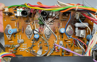
Power amplifier/power supply board - before and after

Sony STR-7065_Power Amplifier & Power Supply Board_before servicing

Sony STR-7065_Power Amplifier & Power Supply Board_after servicing

Control Board

The control amplifier board is quite difficult to service due to the many wires that block access to electronic components. Also, several electrolytic capacitors on this board are located too close to the front panel and are difficult to get for replacement.

Pre-Amplifier Circuit

The pre-amplifier circuit has 2 solid tantalum capacitors (C501, C551) installed in the input signal path, 2 low leakage e-caps (C502, C552) installed in the feedback loop, 2 low leakage e-caps (C508 C558) installed in the output signal path, one aluminum electrolytic capacitor C810 installed in the bias loop, and 2 filtering aluminum e-caps (C811, C812).

The original solid tantalum and two low leakage capacitors (C502, C552) were replaced with modern low leakage Nichicon UKL caps. The other two low leakage e-caps installed in the output signal path were replaced with high-quality film polyester WIMA caps. The original e-cap C810 was also replaced with a film polyester WIMA cap. The remaining filtering capacitors are replaced with low impedance Nichicon UPW capacitors.

Test results on original capacitors removed from the pre-amplifier circuit:

C501: rated capacitance – 3.3uF, measured – 3.5uF, ESR – 0.92Ω, deviation: +6%
C551: rated capacitance – 3.3uF, measured – 3.6uF, ESR – 0.94Ω, deviation: +9%
C502: rated capacitance – 33uF, measured – 37uF, ESR – 1.12Ω, deviation: +12%
C552: rated capacitance – 33uF, measured – 35uF, ESR – 1.27Ω, deviation: +6%
C508: rated capacitance – 0.47uF, measured – 0.46uF, ESR – N/A, deviation: -2%
C558: rated capacitance – 0.47uF, measured – 0.51uF, ESR – N/A, deviation: +9%
C810: rated capacitance – 0.47uF, measured – 0.49uF, ESR – N/A, deviation: +4%
C811: rated capacitance – 220uF, measured – 222uF, ESR – 0.32Ω, deviation: +1%
C812: rated capacitance – 220uF, measured – 235uF, ESR – 0.26Ω, deviation: +7%

Flat Amplifier Circuit

The flat amplifier circuit has 2 solid tantalum capacitors (C603, C653) installed in the input signal path, 4 aluminum electrolytic capacitors (C604, C654, C608, C658) installed in the input signal path, 6 aluminum e-caps (C613, C663, C618, C668, C619, C669) installed in the output signal path, 2 aluminum e-caps (C609, C659) installed in the feedback loop, one aluminum electrolytic capacitor C813 installed in the bias loop, and 2 filtering aluminum e-caps (C814, C815).

The original solid tantalum capacitors, and all ordinary aluminum e-caps installed in the signal path were replaced with low leakage Nichicon UKL caps. The original e-cap C813 was replaced with a film polyester WIMA cap. The remaining filtering capacitors are replaced with low impedance Nichicon UPW capacitors.

Test results on original capacitors removed from the plat amplifier circuit:

C603: rated capacitance – 3.3uF, measured – 3.5uF, ESR – 0.86Ω, deviation: +6%
C653: rated capacitance – 3.3uF, measured – 3.5uF, ESR – 0.98Ω, deviation: +6%
C604: rated capacitance – 3.3uF, measured – 4.1uF, ESR – 2.6Ω, deviation: +24%
C654: rated capacitance – 3.3uF, measured – 3.9uF, ESR – 2.4Ω, deviation: +18%
C608: rated capacitance – 10uF, measured – 12uF, ESR – 0.89Ω, deviation: +20%
C658: rated capacitance – 10uF, measured – 12uF, ESR – 1.03Ω, deviation: +20%
C609: rated capacitance – 47uF, measured – 49uF, ESR – 1.36Ω, deviation: +4%
C659: rated capacitance – 47uF, measured – 51uF, ESR – 1.29Ω, deviation: +9%
C613: rated capacitance – 3.3uF, measured – 3.7uF, ESR – 2.71Ω, deviation: +12%
C663: rated capacitance – 3.3uF, measured – 4.4uF, ESR – 2.12Ω, deviation: +33%
C618: rated capacitance – 3.3uF, measured – 4.1uF, ESR – 1.94Ω, deviation: +24%
C668: rated capacitance – 3.3uF, measured – 3.8uF, ESR – 1.89Ω, deviation: +15%
C619: rated capacitance – 3.3uF, measured – 3.8uF, ESR – 1.73Ω, deviation: +15%
C669: rated capacitance – 3.3uF, measured – 3.6uF, ESR – 2.21Ω, deviation: +9%
C813: rated capacitance – 1uF, measured – 1.2uF, ESR – 1.65Ω, deviation: +20%
C814: rated capacitance – 100uF, measured – 112uF, ESR – 0.42Ω, deviation: +12%
C815: rated capacitance – 100uF, measured – 118uF, ESR – 0.41Ω, deviation: +18%

Noise Elimination Circuit

The noise elimination circuit for the tuner section has 2 aluminum electrolytic capacitors: C809 and C823. I replaced them with low leakage Nichicon UKL caps.

Test results on original capacitors removed from the noise elimination circuit:

C809: rated capacitance – 3.3uF, measured – 3.7uF, ESR – 2.62Ω, deviation: +12%
C823: rated capacitance – 3.3uF, measured – 4.1uF, ESR – 1.96Ω, deviation: +24%

Audio Muting Circuit

The audio muting circuit has 2 aluminum electrolytic capacitors: C807 and C808. I replaced them with low impedance Nichicon UPW capacitors.

Test results on original capacitors removed from the audio muting circuit:

C807: rated capacitance – 100uF, measured – 115uF, ESR – 0.93Ω, deviation: +15%
C808: rated capacitance – 47uF, measured – 61uF, ESR – 0.42Ω, deviation: +30%

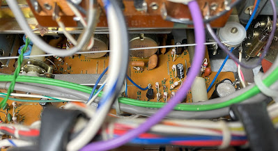
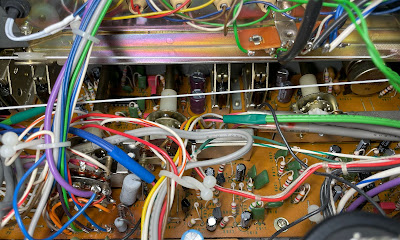
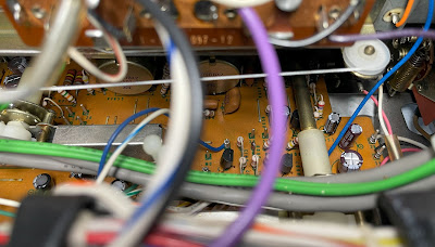
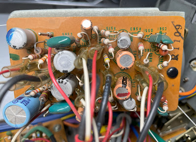
Below are a couple of photos of the control board before and after service (sorry, due to a bunch of different wires, I was not able to take better pictures of this board).

Control board - before servicing

Sony STR-7065_Control Board_01_before servicing

Sony STR-7065_Control Board_02_before servicing

Control board - after servicing

Sony STR-7065_Control Board_01_after servicing

Sony STR-7065_Control Board_02_after servicing

Microphone Amplifier Board

The microphone amplifier board has 2 solid tantalum capacitors (C510 & C560), 4 low leakage e-caps (C512, C513, C562, C563), and 6 aluminum electrolytic capacitors (C514, C516, C564, C566, C820, C821). The original solid tantalum and low leakage capacitors installed in the signal path were replaced with modern low leakage Nichicon UKL caps. The remaining aluminum e-caps were replaced with low impedance Nichicon UPW capacitors.

Test results on original capacitors removed from the microphone amplifier board:

C510: rated capacitance – 3.3uF, measured – 3.5uF, ESR – 2.6Ω, deviation: +6%
C560: rated capacitance – 3.3uF, measured – 3.0uF, ESR – 3.1Ω, deviation: -9%
C512: rated capacitance – 33uF, measured – 38uF, ESR – 0.94Ω, deviation: +15%
C562: rated capacitance – 33uF, measured – 38uF, ESR – 0.96Ω, deviation: +15%
C513: rated capacitance – 3.3uF, measured – 4.9uF, ESR – 2.1Ω, deviation: +48%
C563: rated capacitance – 3.3uF, measured – 4.8uF, ESR – 2.2Ω, deviation: +45%
C514: rated capacitance – 100uF, measured – 115uF, ESR – 0.48Ω, deviation: +15%
C564: rated capacitance – 100uF, measured – 117uF, ESR – 0.38Ω, deviation: +17%
C516: rated capacitance – 10uF, measured – 10uF, ESR – 1.1Ω, deviation: 0%
C566: rated capacitance – 10uF, measured – 10uF, ESR – 1.3Ω, deviation: 0%
C820: rated capacitance – 47uF, measured – 48uF, ESR – 1.12Ω, deviation: +2%
C821: rated capacitance – 220uF, measured – 194uF, ESR – 0.28Ω, deviation: -12%

Microphone amplifier board - before and after

Sony STR-7065_Microphone Amplifier Board_before servicing

Sony STR-7065_Microphone Amplifier Board_after servicing

Dial Cord Restringing

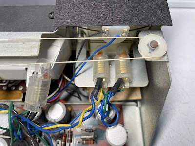
The old dial string in this unit was loosened. I replaced it with a new dial cord (the most tedious job on any vintage receiver).

The old and new dial cord

Sony STR-7065_Dial Cord_old

Sony STR-7065_Dial Cord_new

Dial, Meter, and Stereo Indicator Lamps

The old dial incandescent lamps were replaced with new warm white LED lamps (festoon type). The old meter lamps were also replaced with new warm white LED lamps (fuse type). Finally, the burned stereo indicator lamp was replaced with a new incandescent lamp.

New LED meter lamps

Sony STR-7065_Meter Lamps_new LED

New incandescent stereo indicator lamp

Sony STR-7065_Stereo Indicator Lamp_new incandescent

Power Amplifier Adjustment

The Bias is measured across two emitter resistors: R718 & R719 (left channel) and R768 & R769 (right channel). According to the service manual, it should be adjusted to 50mV on each channel with trimming resistors RT701 and RT751.

As I mentioned earlier, the STR-7065 does not have trimmers to adjust the DC offset on each channel. I was able to bring it down to an acceptable level by replacing the OEM Sony transistors in the differential amplifier with new close-matched Fairchild transistors (see the "Power Amplifier/Power Supply Board" section for details).

Bias on the left and right channels after restoration

Sony STR-7065_Bias_left channel

Sony STR-7065_Bias_right channel

DC offset on the left and right channels after restoration

Sony STR-7065_DC Offset_left channel

Sony STR-7065_DC Offset_right channel

Output Power Test

The final output power test was performed at the end of my restoration. The receiver was loaded with a low inductance 8Ω/100W dummy resistor for each channel. The oscilloscope was connected across the speaker terminals and a sine-wave signal of 1kHz was applied to the AUX jacks. The output sine-wave signal was perfectly symmetrical on both channels with no clipping up to 23.05 VRMS (left channel) and 23.33 VRMS (right channel). It corresponds to the output power of 66.4W on the left channel and 68.0W on the right channel.

Output power test

Sony STR-7065_Output Power Test

As usual, all the knobs and the front panel were gently cleaned in warm water with dish soap. All controls have been cleaned with DeoxIT 5% contact cleaner and lubricated with DeoxIT FaderLube 5% spray. The wood case was treated with Howard's Restor-A-Finish.

The final result can be seen in the photos below. It looks and sounds great! Please watch a short demo video at the end of this post. Thank you for reading.

Sony STR-7065 - after restoration

Sony STR-7065_after restoration

Sony STR-7065_after restoration_with old parts

Demo video after repair & restoration

Tuesday, August 1, 2023

JVC VR-5551 Receiver Restoration

Unit: AM/FM Stereo Receiver
Manufacturer: JVC
Model: VR-5551
SN: 13402565

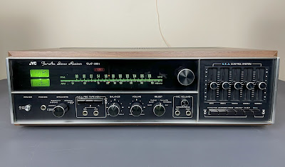
A pretty rare JVC VR-5551 stereo receiver is on my bench today. This model was manufactured from 1972 to 1975 and held the top position in JVC's production line, featuring the VR-5551, VR-5541, VR-5521, VR-5511, and VR-5501. It delivers 50 watts per channel into 8 ohms with no more than 0.5% total harmonic distortion. The damping factor at 8 ohm is 50. The retail price in 1972 was approximately $450.

An interesting feature of this model is the five-band version of the Sound Effects Amplifier (U.S. Patent No. 3,566,294 issued February 1971). The five sliders are calibrated to boost or cut up to 12dB over frequency bands with center reference frequencies of 40Hz, 250Hz, 1kHz, 5kHz, and 15kHz, respectively. These sliders operate continuously, registering clicks every 2 dB on the scale. Below the SEA section are six pushbuttons for FM muting, loudness, mono mode, low filter, high filter, and SEA defeat. 

The other features of the VR-5551 are a black face dial with a "Bull's eye" FM dial pointer, two tuning meters, front-panel tape recording & playback jacks for recording with or without SEA, left and right microphone inputs with their own master level control, a special protector circuit, and a luxurious walnut wooden cabinet.

The VR-5551 receiver is easy to service, with the exception of two double-soldered PCBs, to which access is restricted.

JVC_VR-5551_after restoration

Power Supply Board (TAP-113)

The power supply board has 7 aluminum electrolytic capacitors: C801, C802, C804, C806, C807, C808, and C810. All of them were replaced with low impedance Nichicon UPW/UPM caps. The old glue around some large e-caps was carefully removed. This glue often corrodes capacitor leads and even can damage the PCB. I highly recommend removing it before installing new capacitors.

The original e-caps were tested with an Atlas ESR70 capacitance meter; the results are below.

Test results on original capacitors removed from the power supply board:

C801: rated capacitance – 470uF, measured – 497uF, ESR – 0.05Ω, deviation: +6%
C802: rated capacitance – 470uF, measured – 494uF, ESR – 0.06Ω, deviation: +5%
C804: rated capacitance – 470uF, measured – 576uF, ESR – 0.03Ω, deviation: +23%
C806: rated capacitance – 470uF, measured – 576uF, ESR – 0.05Ω, deviation: +23%
C807: rated capacitance – 470uF, measured – 591uF, ESR – 0.07Ω, deviation: +26%
C808: rated capacitance – 220uF, measured – 245uF, ESR – 0.12Ω, deviation: +11%
C810: rated capacitance – 470uF, measured – 580uF, ESR – 0.12Ω, deviation: +23%

Power supply board - before and after

JVC_VR-5551_Power Supply Board (TAP-113)_before servicing

JVC_VR-5551_Power Supply Board (TAP-113)_after servicing

Driver Amplifier Board (TAD-79)

The driver amplifier board is fixed in a slot which greatly simplifies the servicing of this board. It has one axial (C719) and 12 radial (C701, C702, C703, C704, C707, C708, C709, C710, C711, C712, C718) aluminum electrolytic capacitors. The e-caps C701 and C702 installed in the input signal path were replaced with high-quality film polyester WIMA caps. Other two e-caps C703 and C704 installed in the signal path were replaced with modern low leakage Nichicon UKL caps. The original axial capacitor C719 was replaced with a Vishay axial e-cap (500D series). And the remaining aluminum e-caps were replaced with low impedance Nichicon UPW/UPM caps.

Test results on original capacitors removed from the driver amplifier board:

C701: rated capacitance – 1uF, measured – 1.3uF, ESR – 1.32Ω, deviation: +30%
C702: rated capacitance – 1uF, measured – 1.2uF, ESR – 1.31Ω, deviation: +20%
C703: rated capacitance – 33uF, measured – 40uF, ESR – 0.45Ω, deviation: +21%
C704: rated capacitance – 33uF, measured – 40uF, ESR – 0.49Ω, deviation: +21%
C707: rated capacitance – 100uF, measured – 119uF, ESR – 0.22Ω, deviation: +19%
C708: rated capacitance – 100uF, measured – 113uF, ESR – 0.24Ω, deviation: +13%
C709: rated capacitance – 100uF, measured – 126uF, ESR – 0.89Ω, deviation: +26%
C710: rated capacitance – 100uF, measured – 131uF, ESR – 0.21Ω, deviation: +31%
C711: rated capacitance – 47uF, measured – 57uF, ESR – 1.22Ω, deviation: +21%
C712: rated capacitance – 47uF, measured – 58uF, ESR – 0.59Ω, deviation: +23%
C717: rated capacitance – 100uF, measured – 119uF, ESR – 0.13Ω, deviation: +19%
C718: rated capacitance – 100uF, measured – 116uF, ESR – 0.14Ω, deviation: +16%
C719: rated capacitance – 10uF, measured – 12uF, ESR – 1.58Ω, deviation: +20%

The prone-to-failure Hitachi 2SC458LG transistor installed in positions X701, X702, X709, X710, X711, and X712  was replaced with a low-noise Fairchild KSC1845 transistor. Watch the pinout on replacement transistors. The original transistor is BCE and the new one is ECB.

Driver amplifier board - before and after

JVC_VR-5551_Driver Amplifier Board (TAD-79)_before servicing

JVC_VR-5551_Driver Amplifier Board (TAD-79)_after servicing

Equalizer Circuit Board (TAE-47)

The equalizer circuit board is also fixed in a separate slot. This board has 11 aluminum electrolytic capacitors: C501, C502, C503, C504, C507, C508, C511, C512, C513, C514, and C521. All e-caps installed in the signal path (C501, C502, C507, C508, C511, C512) were replaced with modern low leakage Nichicon UKL caps to reduce the noise generated in the circuit. The remaining aluminum e-caps were replaced with low impedance Nichicon UPW caps.

Test results on original capacitors removed from the equalizer circuit board:

C501: rated capacitance – 3.3uF, measured – 3.6uF, ESR – 1.1Ω, deviation: +9%
C502: rated capacitance – 3.3uF, measured – 3.5uF, ESR – 0.59Ω, deviation: +6%
C503: rated capacitance – 10uF, measured – 13uF, ESR – 1.65Ω, deviation: +30%
C504: rated capacitance – 10uF, measured – 13uF, ESR – 1.71Ω, deviation: +30%
C507: rated capacitance – 10uF, measured – 12uF, ESR – 0.78Ω, deviation: +20%
C508: rated capacitance – 10uF, measured – 12uF, ESR – 0.77Ω, deviation: +20%
C511: rated capacitance – 10uF, measured – 12uF, ESR – 0.56Ω, deviation: +20%
C512: rated capacitance – 10uF, measured – 12uF, ESR – 0.68Ω, deviation: +20%
C513: rated capacitance – 100uF, measured – 120uF, ESR – 0.27Ω, deviation: +20%
C514: rated capacitance – 100uF, measured – 115uF, ESR – 0.26Ω, deviation: +15%
C521: rated capacitance – 10uF, measured – 11uF, ESR – 0.72Ω, deviation: +10%

All notorious Hitachi 2SC458LG transistors installed in positions X501 thru X504 were replaced with low-noise Fairchild KSC1845 transistors. Again, watch the pinout on replacement transistors. The original transistor is BCE and the new one is ECB.

Equalizer circuit board - before and after

JVC_VR-5551_Equalizer Circuit Board (TAE-47)_before servicing

JVC_VR-5551_Equalizer Circuit Board (TAE-47)_after servicing

SEA Circuit Board (TAC-147)

The SEA circuit board in this receiver is a double-soldered PCB. This type of PCB is very difficult to service especially if the other side is not accessible. Fortunately, this board has only 4 electrolytic capacitors to be replaced: C621, C522, C623, and C624. I replaced two e-caps with a nominal capacitance of 0.62uF with film polyester WIMA caps. The other two e-caps were replaced with low leakage Nichicon UKL caps.

Test results on original capacitors removed from the SEA circuit board:

C621: rated capacitance – 10uF, measured – 12uF, ESR – 0.34Ω, deviation: +20%
C622: rated capacitance – 10uF, measured – 11uF, ESR – 0.68Ω, deviation: +10%
C623: rated capacitance – 0.68uF, measured – 0.66uF, ESR – N/A, deviation: -3%
C624: rated capacitance – 0.68uF, measured – 0.62uF, ESR – N/A, deviation: -9%

SEA circuit board - before and after

JVC_VR-5551_SEA Circuit Board (TAC-147)_before servicing

JVC_VR-5551_SEA Circuit Board (TAC-147)_after servicing

Microphone Amplifier Board (TAC-150)

The microphone amplifier board has 7 aluminum electrolytic capacitors: C661, C662, C663, C664, C665, C666, and C671. I replaced two e-caps (C661 & C662) installed in the input signal path with film polyester WIMA caps. All other e-caps were replaced with low impedance Nichicon UPW capacitors.

Test results on original capacitors removed from the microphone amplifier board:

C661: rated capacitance – 1uF, measured – 1.4uF, ESR – 1.24Ω, deviation: +40%
C662: rated capacitance – 1uF, measured – 1.3uF, ESR – 1.34Ω, deviation: +30%
C663: rated capacitance – 10uF, measured – 13uF, ESR – 1.42Ω, deviation: +30%
C664: rated capacitance – 10uF, measured – 13uF, ESR – 1.53Ω, deviation: +30%
C665: rated capacitance – 100uF, measured – 119uF, ESR – 0.42Ω, deviation: +19%
C666: rated capacitance – 100uF, measured – 111uF, ESR – 0.26Ω, deviation: +11%
C671: rated capacitance – 10uF, measured – 12uF, ESR – 1.22Ω, deviation: +20%

This board also has 4 notorious Hitachi 2SC458LG transistors installed in positions X651 thru X654. I replaced them with low-noise Fairchild KSC1845 transistors. Again, watch the pinout on replacement transistors. The original transistor is BCE and the new one is ECB.

Microphone amplifier board - before and after

JVC_VR-5551_Microphone Amplifier Board (TAC-150)_before servicing

JVC_VR-5551_Microphone Amplifier Board (TAC-150)_after servicing

Switch Assembly (TAC-148)

The switch assembly is another double-soldered PCB in this receiver.  I recommend removing this board from the chassis before servicing. Otherwise, there is a high probability of burning the dial cord behind this board.

The switch assembly has 11 aluminum electrolytic capacitors: C605, C606, C607, C608, C609, C610, C611, C612, C613, C614, and C619. I replaced two e-caps (C605 & C606) installed in the input signal path with film polyester WIMA caps. The other e-caps (C607, C608, C611, C612) installed in the signal path were replaced with modern low leakage Nichicon UKL caps. And the remaining aluminum e-caps were replaced with low impedance Nichicon UPW caps.

Test results on original capacitors removed from the switch assembly:

C605: rated capacitance – 1uF, measured – 1.2uF, ESR – 2.1Ω, deviation: +20%
C606: rated capacitance – 1uF, measured – 1.2uF, ESR – 2.2Ω, deviation: +20%
C607: rated capacitance – 33uF, measured – 42uF, ESR – 0.72Ω, deviation: +27%
C608: rated capacitance – 33uF, measured – 40uF, ESR – 0.92Ω, deviation: +21%
C609: rated capacitance – 10uF, measured – 12uF, ESR – 0.64Ω, deviation: +20%
C610: rated capacitance – 10uF, measured – 12uF, ESR – 0.98Ω, deviation: +20%
C611: rated capacitance – 33uF, measured – 39uF, ESR – 0.43Ω, deviation: +18%
C612: rated capacitance – 33uF, measured – 38uF, ESR – 0.56Ω, deviation: +15%
C613: rated capacitance – 33uF, measured – 38uF, ESR – 2.6Ω, deviation: +15%
C614: rated capacitance – 33uF, measured – 38uF, ESR – 2.4Ω, deviation: +15%
C619: rated capacitance – 10uF, measured – 12uF, ESR – 1.1Ω, deviation: +20%

Switch assembly - before and after

JVC_VR-5551_Switch Assembly (TAC-148)_before servicing

JVC_VR-5551_Switch Assembly (TAC-148)_after servicing

Main Filter and Two Coupling Capacitors

The original filter capacitor in this unit was replaced with a new Kemet screw terminal electrolytic capacitor. Additionally, the original coupling capacitors were replaced with Nichicon LKG capacitors. The LKG series was specifically designed for high-grade audio equipment and, in my opinion, is the best replacement option for the original filter and/or coupling capacitors available on the market. The new Nichicon LKG e-caps have the same diameter as the original ones but are shorter in length. As a result, the same clamps can be used to attach them to the chassis.

Test results on the original filter and coupling capacitors:

C4: rated capacitance – 2200uF, measured – 2782uF, ESR – 0.08Ω, deviation: +27%
C4: rated capacitance – 2200uF, measured – 2380uF, ESR – 0.07Ω, deviation: +8%
C5: rated capacitance – 2200uF, measured – 2417uF, ESR – 0.07Ω, deviation: +10%

Dial and Meter Lamps

The dial and meter lamps in this model are easily accessible. I replaced them with new incandescent lamps (screw base, 300mA, 8V).

The Stereo indicator lamp was also replaced with a new incandescent lamp (4mm, 40mA, 6V). 

Dial lamps - screw base

JVC_VR-5551_Dial Lamps

Meter lamps - screw base

JVC_VR-5551_Meter Lamps

Center Voltage and Idling Current Adjustments

There is some confusion in the service manual regarding the adjustment of the center voltage and idling current. The service manual states that the center voltage on each channel must be adjusted with a trimming resistor R102, as shown in the circuit on page 9. Additionally, the idling current should be adjusted using a trimming resistor R101, also detailed in the circuit on the same page. However, the schematic diagram displays these trimming resistors as R719/R720 (center voltage) and R735/R736 (idling current). Furthermore, the driver amplifier board being serviced lacks trimming resistors R735 and R736 to adjust the idling current. Instead, two resistors (with a nominal resistance of 8.2Ω each) were factory soldered in positions R735 and R736. This makes the adjustment of the idling current problematic in this unit. It appears that JVC implemented this as a cost-reduction solution during the production of this model.

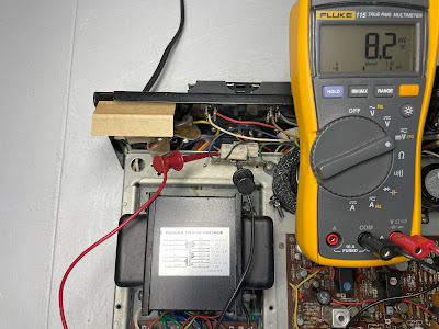
To adjust the center voltage on each channel, it must be set to half of the +B1 voltage. The +B1 voltage can be measured between pin #6 on the driver amplifier board and the ground (or across the main filter capacitor). In this unit, the measured +B1 voltage was 84.1 DC. The center voltage is measured between the positive lead of coupling capacitor C4/C5 (2200uF/63V) and the ground. I adjusted the center voltage on each channel to half of the measured +B1 voltage using trimming resistors R719/R720.

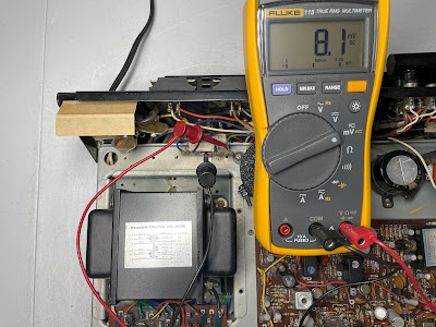
According to the service manual, the idling current on each channel must be between 10mA to 20mA. The idling current can be calculated by measuring the voltage drop across the emitter resistor R5 (R6). Since the nominal resistance of R5 (R6) is 0.5Ω, the voltage drop across each resistor should be between 5mV to 10mV. I measured the voltage drop across emitter resistor R5 (left channel), and it was close to ~11mV. However, the measured voltage drop across emitter resistor R6 (right channel) was close to ~32mV, which is about three times higher than the recommended value in the manual. As I mentioned earlier, this particular unit has no trimming resistor to adjust the idling current. So, the only way to adjust it is to replace the single resistor factory soldered in position R736. I replaced it with a KOA Speer metal film resistor with a nominal resistance of 3.32Ω, and it reduced the idling current on the right channel to ~16mA (the measured voltage drop across R736 is ~8mV).

+B1 voltage measured between pin #6 and ground

JVC_VR-5551_B1 Voltage

The center voltage on the left and right channels after restoration

JVC_VR-5551_Center Voltage_left channel

JVC_VR-5551_Center Voltage_right channel

Bias on the left and right channels after restoration

JVC_VR-5551_Bias_left channel

JVC_VR-5551_Bias_right channel

Output Power Test

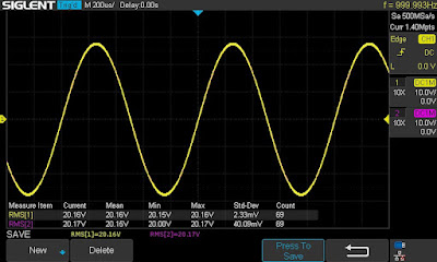
The final output power test was performed at the end of my restoration. The receiver was loaded with a low inductance 8Ω/100W dummy resistor for each channel. The oscilloscope was connected across the speaker terminals and a sine-wave signal of 1kHz was applied to the AUX jacks. The output sine-wave signal was perfectly symmetrical on both channels with no clipping up to 20.16 VRMS (left channel) and 20.17 VRMS (right channel). It corresponds to the output power of 50.8W on the left channel and 50.9W on the right channel.

Output power test

JVC_VR-5551_Output Power Test

As usual, all the knobs and the front panel were gently cleaned in warm water with dish soap. All controls have been cleaned with DeoxIT 5% contact cleaner and lubricated with DeoxIT FaderLube 5% spray.

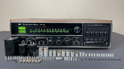
The final result can be seen in the photos below. This model looks and sounds awesome! Please watch a short demo video at the end of this post. Thank you for reading.

JVC VR-5551 - after restoration
JVC_VR-5551_after restoration

JVC_VR-5551_after restoration_with old parts

Demo video after repair & restoration