Unit: AM/FM Stereo Receiver
Manufacturer: Pioneer
Model: SX-650
SN: WL3633228S
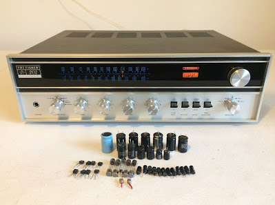
Today I'm showcasing a Pioneer SX-650 receiver that came in for restoration. The SX-650 was manufactured from 1976 to 1978. It produces 35 watts per channel into 8 ohms with no more than 0.3% total harmonic distortion. The list price in 1976 was around $300. This particular unit came in with several faulty components. However, the receiver is still in excellent cosmetic condition. The wood case, faceplate, and all knobs are almost flawless. It is certainly worth restoring. According to the Pioneer database, this unit was manufactured in December 1976.
Initial Troubleshooting
The previous owner told me that one channel is highly distorted and the other channel sounds very weak. First of all, I decided to check the operating voltages on Sanken SP-40W Power Modules to make sure that nothing was wrong with them. There is no modern substitution for those modules and the new modules available on eBay are usually counterfeit from China. A quick test showed that all measured voltages on both modules were very close to the reference voltages on the schematic. Well, at least these power modules are not burned out.
Test results on Sanken SP-40W power modules:
pin 1: schematic: 36V, left channel: 36.2V, right channel: 36.1V
pin 2: schematic: 1.2V, left channel: 1.3V, right channel: 1.3V
pin 3: schematic: 65mV, left channel: 63mV, right channel: 58mV
pin 4: schematic: 33mV, left channel: 37mV, right channel: 31mV
pin 5: schematic: -36V, left channel: -36.1V, right channel: -36.1V
pin 6: schematic: -1.2V, left channel: -1.2V, right channel: -1.2V
pin 7: schematic: -6mV, left channel: 9.8mV, right channel: 6.2mV
pin 8: schematic: N/A, left channel: 0V, right channel: 0V
The next test I completed was to trace the input signal through the balance/volume control, tone control, power amplifier - 1, power amplifier - 2, and down to the speaker's terminals. This test will show me where the signal is distorted or attenuated. So, I connected my function generator to the AUX terminals, applied a sine-wave signal of 1 kHz, and traced the input signal with my oscilloscope throughout all boards down to the speaker's terminals. Surprisingly but the sine-wave signal was clear and without any distortion throughout all boards. I connected my cell phone to the AUX terminals and the receiver played music with a crystal clear sound. It looks like the amplifier in this unit has no issues.
So, the last step was to check the tuner performance. I connected the FM antenna to 300 Ohm terminals of SX-650 and switched to FM broadcasts. Tuned the knob to the local FM station and immediately realized that the left channel was very weak and the right channel was highly distorted. At the same time, the signal strength was very strong and the stereo indicator lamp came on. Well, there is definitely some issue in the tuner circuit.
I turned off the receiver and tested all transistors and diodes in the tuner circuit. All semiconductor devices were normal. Then, I turned on the receiver again and checked the operating voltages on all transistors and integrated circuits (ICs). The measured voltages on all six transistors Q1 thru Q4, Q7, and Q8 were very close to the reference voltages on the schematic. Two ICs Q5 and Q9 also had the correct operating voltages on all pins. However, the integrated circuit Q6 was in question. The measured voltage on pins 4, 6, and 7 didn't match the reference voltage on the schematic.
Test results on integrated circuit Q6:
pin 1: schematic: 14.0V, measured: 14.0V
pin 2: schematic: 3.0V, measured: 3.1V
pin 3: schematic: 7.5V, measured: 7.7V
pin 4: schematic: 11.0V, measured: 4.8V
pin 5: schematic: 11.0V, measured: 11.2V
pin 6: schematic: 7.3V, measured: 9.5V
pin 7: schematic: 7.3V, measured: 4.9V
pin 8: schematic: ground, measured: 0V
pin 9: schematic: 0.1V, measured: 1.0V
pin 10: schematic: 2.3V, measured: 2.5V
pin 11: schematic: N/A, measured: 2.4V
pin 12: schematic: N/A, measured: 0V
pin 13: schematic: 2.2V, measured: 2.5V
pin 14: schematic: 2.4V, measured: 2.5V
pin 15: schematic: 2.4V, measured: 2.5V
pin 16: schematic: 3.0V, measured: 3.2V
The integrated circuit Q6 (HA1196) installed on Pioneer SX-650 is an MPX decoder. Pins 4 and 5 are the left and right channel outputs, respectively. And pins 6 and 7 provide feedback control. The sound from the left channel is very weak when the receiver is switched to FM broadcasts. It makes sense since the measured voltages on both pins (4 and 7) don't match with the reference voltages on the schematic. The right channel has a sound but it is highly distorted. It also makes sense since the measured voltage on pin 5 is close to the reference voltage but there is a problem with feedback control on pin 6. So, it looks like a faulty IC. I unsoldered the IC Q6 from the board and installed a new HA1196 chip on the 16-pin DIP socket. Then, I turned on the receiver, tuned the knob to the local FM station, and... The left channel was still very weak and the right channel was still highly distorted. Huh! It looks like there is another faulty component on the tuner board. I carefully inspected all passive electronic components around the HA1196 chip and found that the polystyrene film capacitor C41 (510pF) is faulty. I replaced it with a new polystyrene cap and there you go! The clear sound from FM broadcasting was restored. No more distortions. The measured voltages on all pins match with the reference voltages on the schematic. Yep, the troubleshooting of the tuner circuit is always a tricky task. Now it's time to service other boards.
Test results on integrated circuit Q6 after HA1196 chip and capacitor C41 replacement:
pin 1: schematic: 14.0V, measured: 14.0V
pin 2: schematic: 3.0V, measured: 3.1V
pin 3: schematic: 7.5V, measured: 7.7V
pin 4: schematic: 11.0V, measured: 11.1V
pin 5: schematic: 11.0V, measured: 11.1V
pin 6: schematic: 7.3V, measured: 6.7V
pin 7: schematic: 7.3V, measured: 6.7V
pin 8: schematic: ground, measured: 0V
pin 9: schematic: 0.1V, measured: 1.0V
pin 10: schematic: 2.3V, measured: 2.5V
pin 11: schematic: N/A, measured: 2.4V
pin 12: schematic: N/A, measured: 0V
pin 13: schematic: 2.2V, measured: 2.3V
pin 14: schematic: 2.4V, measured: 2.5V
pin 15: schematic: 2.4V, measured: 2.5V
pin 16: schematic: 3.0V, measured: 3.3V
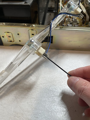
Old and new integrated circuit Q6 (HA1196)
16 pin DIP socket for integrated circuit Q6
New HA1196 chip installed on the socket
Power Amp - 1 Board
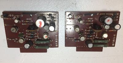
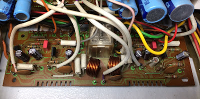
The power amp - 1 board (#GWH 101) has two tantalum capacitors C1 and C2 installed in the signal path. I replaced them with high-quality film polyester WIMA MKS2 caps. Other 6 e-caps C7 thru C10, C13, and C14 were replaced with low impedance and high-reliability Nichicon UPW caps. The protection relay S1 installed on this board is very clean inside and I didn't notice any contact degradation. So, I didn't replace it. The modern substitution for this relay is Omron MY4-02-DC24.
Power Amp - 1 (#GWH 101) - before and after
Power Amp - 2 Board
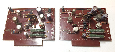
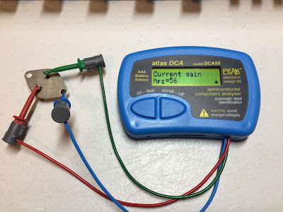
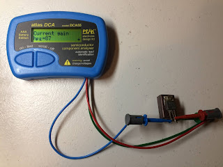
The original coupling capacitors C21 and C22 installed on the power amp - 2 board (#GWR 101) are sky blue Sanyo electrolytic caps. These e-caps become very leaky over time and should be always replaced in any vintage gear. For more information about sky blue Sanyo e-caps refer to my previous post on Pioneer SX-828 restoration. I replaced them with high-quality film polyester Kemet caps. The other 15 e-caps installed on this board were replaced with new Nichicon UPW/UPM caps. I also removed and tested two transistors Q7 and Q8 mounted on the heat sinks with Atlas DCA55 semiconductor analyzer. Both transistors passed the test and the measured DC current gain was in spec according to the datasheet. I applied a new silicone thermal compound between each transistor and the heat sink before installation on the board.
Sky blue Sanyo coupling capacitors C21 and C22 - replaced with film polyester Kemet caps
Power Amp - 2 (#GWR 101) - before and after
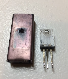
Transistors Q7 and Q8 were removed from the board and tested with Atlas DCA55 semiconductor analyzer
The old thermal grease is almost completely dried out
Tone Control Board
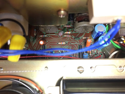
The tone control board (#AWG049) has only 8 electrolytic capacitors but this board is not easily accessible to work on. I would strongly recommend removing the faceplate and the dial frame before servicing this board. I don't think it would be possible to install any new electronic components without removing the faceplate and the dial frame. Even when these two parts are removed it is still a bit tricky to install some particular capacitors.
This board has two tantalum capacitors C1 and C2 which were replaced with high-quality film polyester WIMA MKS2 caps. Two low leakage e-caps C13 and C14 were replaced with new low leakage Nichicon UKL caps. The remaining four electrolytic capacitors were replaced with low impedance and high-reliability Nichicon UPW caps.
Faceplate and dial frame removed - Tone control board is behind the pots
Tone control board - before and after - very limited space to work on
Tuner and AF Board
On the board (#AWE075) I replaced all tantalum capacitors C43 thru C50 installed in the signal path after the multiplex decoder circuit. The capacitors C43 and C44 were replaced with low leakage Nichicon UKL caps. Four capacitors C45 thru C48 were replaced with high-quality film polyester Kemet R82 series, and the last two C49 and C50 with film polyester WIMA MKS2 caps.
The phono equalizer and microphone circuits are both a part of the tuner and AF board. The phono equalizer has 8 e-caps: C76, C77, C84, C85, C90, C91, C94, and C95. Four of them C76, C77, C90, and C91 are tantalum caps. I replaced them with low leakage Nichicon UKL caps. The remaining 4 caps were replaced with low impedance and high-reliability Nichicon UPW caps.
The microphone amp has four e-caps: C100, C101, C104, and C105. The e-caps C100 and C104 are tantalum caps and were replaced with high-quality film polyester Kemet R82 and WIMA MKS2 caps, respectively. The remaining 2 caps were replaced with Nichicon UPW caps.
Tuner and AF board - before and after
Phono equalizer circuit - before and after
Microphone amp circuit - before and after - very limited space to work on
Output Power Test
At the end of my restoration, I loaded this receiver with a low inductance 8Ω/100W dummy resistor for each channel, connected my oscilloscope across the speaker terminals, and applied a sine-wave signal of 1 kHz to the AUX jacks. The output sine-wave signal was perfectly symmetrical on both channels with no clipping up to 15.73 VRMS (left channel) and 16.63 VRMS (right channel). So, one can calculate that the output power is (15.73x15.73)/8=31W (left channel) and (16.63x16.63)/8=35W (right channel). It is very close to factory specifications. A very small difference between the left and right channels is attributed to the imperfection/aging of the balance potentiometer. Keep in mind that this baby is almost 43 years old but still in perfect working condition!
Output power test
As usual, all the knobs and the front panel were gently cleaned in warm water with dish soap. All knobs were also slightly polished by Mothers Mag & Aluminum polish to remove some small spots of aluminum oxidation. All pots and switches have been cleaned with DeoxIT 5% contact cleaner and lubricated with DeoxIT FaderLube 5% spray.
The final result is amazing. The receiver looks brand new. The sound is wonderful and it has plenty of power for home stereo needs. Please watch a short demo video at the end of this post. Thank you for reading.
Pioneer SX-650 - before restoration
Pioneer SX-650 - after restoration







_before%20servicing.jpg)
_after%20servicing.jpg)
_before%20servicing.jpg)
_after%20servicing.jpg)
